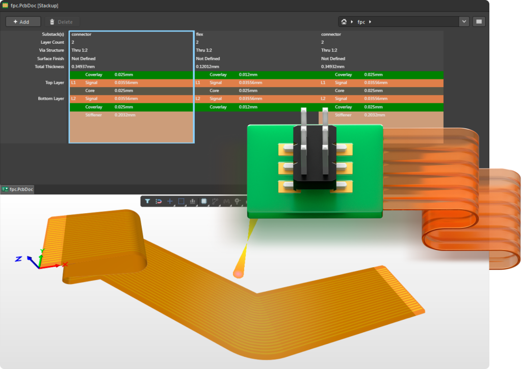
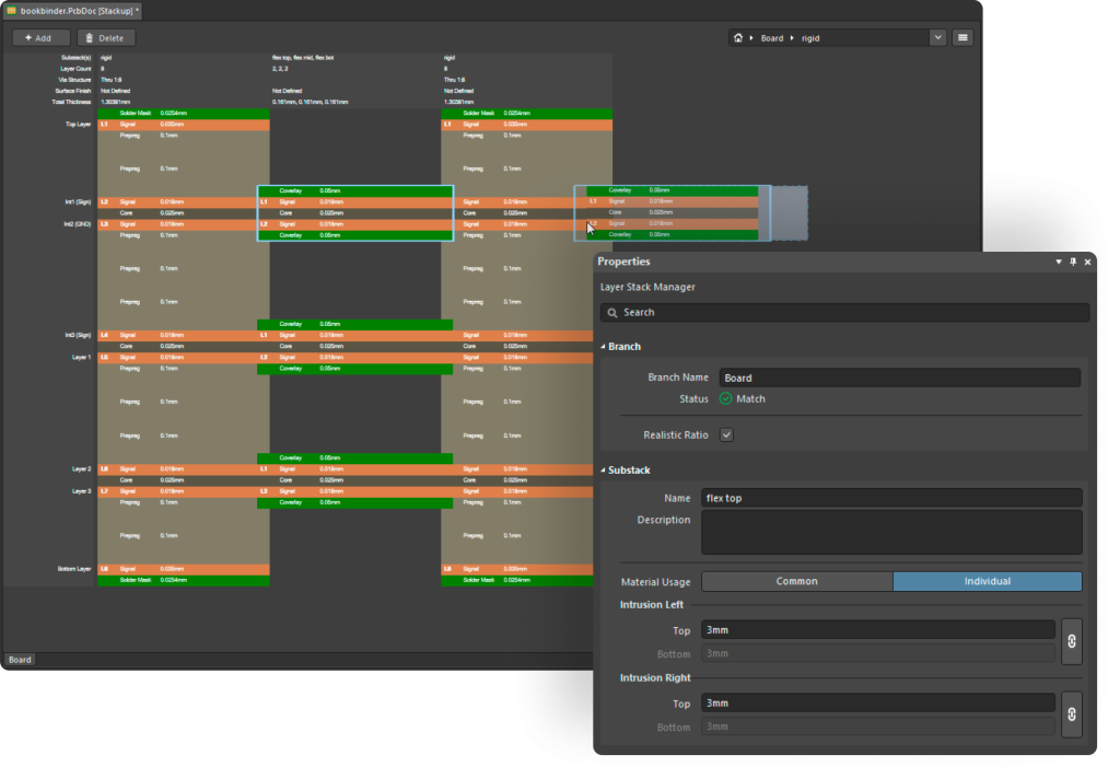
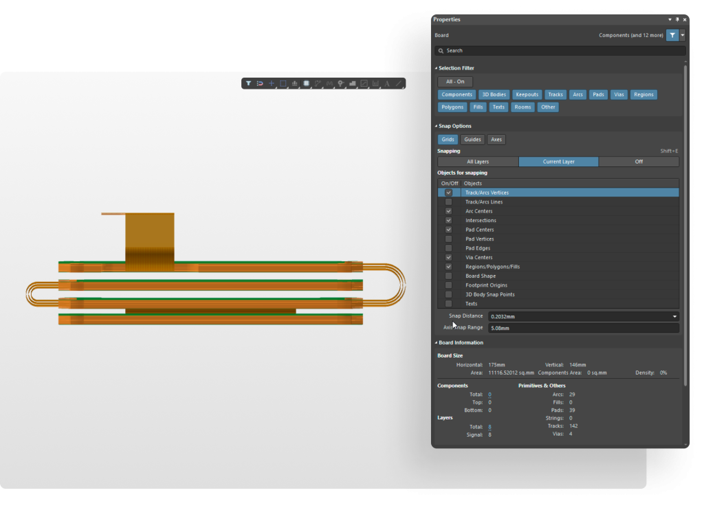
Strona główna » Projektowanie PCB typu Rigid-Flex
Twórz projekty flex i rigid-flex
w zintegrowanym środowisku Altium Designer,
bez ograniczeń i bez potrzeby dodatkowych licencji.
Dodawanie usztywnień, klejów i powłok ochronnych do płytek PCB jest proste i przejrzyste dla producenta. Upraszcza to projektowanie złożonych struktur warstw, ułatwiając zadanie zarówno początkującym, jak i doświadczonym użytkownikom. To narzędzie usprawnia cały proces projektowania, czyniąc nawet skomplikowane zadania łatwiejszymi i zapewniając wysoką jakość wyników. Co więcej, pozwala skutecznie zarządzać kosztami płytek typu rigid-flex, wspierając bardziej ekonomiczne projekty.
Uzyskaj przejrzysty obraz swojej płytki Rigid-Flex dzięki wysokiej jakości wizualizacjom w Altium Designer. Menedżer stosu warstw umożliwia łatwe zrozumienie funkcji każdej warstwy i sekcji elastycznej.
Utilize electrical layers outside the main layer stack specifically for die pins and bond wires. This configuration ensures clear and accurate representation of wire bonding elements, enhancing the reliability and precision of your designs.
Podnieś swoje umiejętności projektowe
i usprawnij proces pracy – wszystko pod okiem doświadczonych ekspertów, którzy pokażą, jak w pełni wykorzystać możliwości programu Altium Designer.
Dowiedz się, jak współpracować z zespołem elektryków, nie rezygnując z wydajności i efektywności.
Jesteś gotowy, aby sprostać wyzwaniom swojej branży?
Skontaktuj się z nami – poznasz nasze rozwiązania i otrzymasz indywidualną poradę od naszych specjalistów. Jesteśmy tutaj, by wspierać Cię w wyborze najskuteczniejszych technologii dopasowanych do Twoich potrzeb.
Świat technologii nie zwalnia. Dzięki naszym rozwiązaniom możesz skupić się na tym, co najważniejsze – na swoim biznesie.