Zdefiniuj na nowo granice PCB dzięki projektowaniu HDI
Spełnij wymagania nowoczesnych, energooszczędnych i kompaktowych PCB dzięki zintegrowanemu środowisku projektowemu w Altium Designer.
Kompleksowe narzędzie do projektowania HDI
Obsługa najnowszych technologii
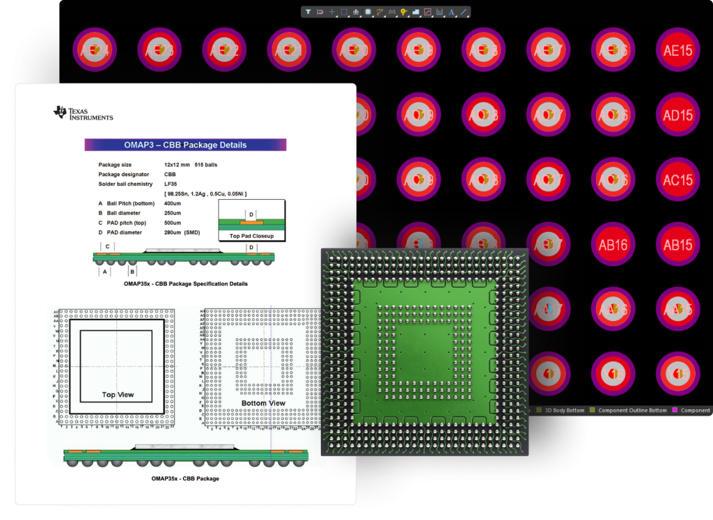
Dzisiejsze zaawansowane komponenty często mają bardzo małe odstępy między wyprowadzeniami, co wymaga stosowania cienkich ścieżek oraz specjalistycznych technik, takich jak via-in-pad czy ślepe przelotki (blind vias). Miniaturyzacja ta stanowi wyzwanie dla tradycyjnego projektowania obwodów, wymagając precyzyjnych i innowacyjnych podejść w celu pełnego wykorzystania ich potencjału.
Maksymalizacja funkcjonalności w projekcie
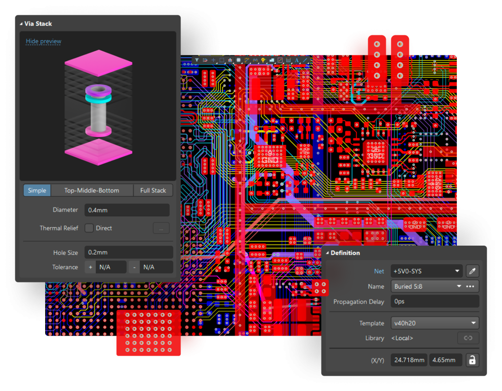
Technologia HDI umożliwia złożone prowadzenie ścieżek i rozmieszczanie przelotek, zwiększając gęstość bez utraty funkcjonalności, co pozwala na tworzenie kompaktowych, a jednocześnie wysoce funkcjonalnych urządzeń.
Najwyższa jakość sygnału
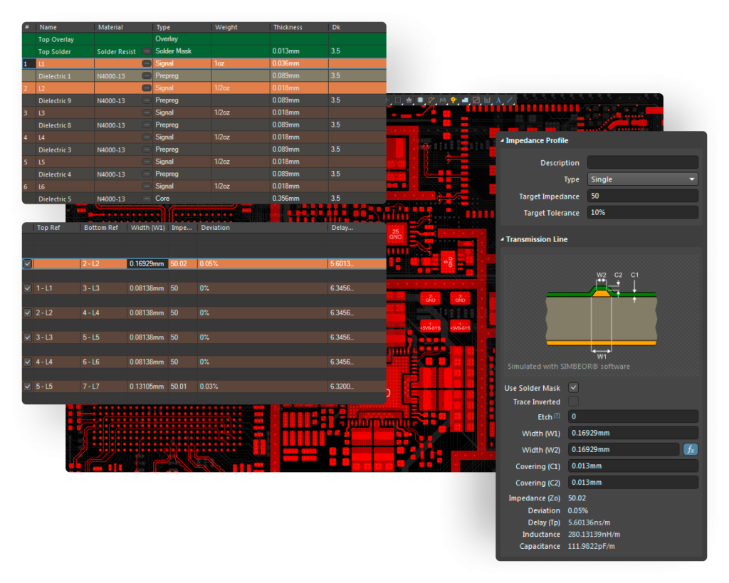
Narzędzia HDI w Altium Designer podnoszą jakość prowadzenia ścieżek poprzez optymalizację sygnału. Kluczowe funkcje to: łagodne prowadzenie ścieżek bez ostrych załamań, kontrola impedancji, minimalna długość połączeń oraz strategiczne rozmieszczenie przelotek w celu redukcji stubów.
Key Capabilities
Electrical Layers for Die Pins
and Bond Wires
Utilize electrical layers outside the main layer stack specifically for die pins and bond wires. This configuration ensures clear and accurate representation of wire bonding elements, enhancing the reliability and precision of your designs.
Utilize electrical layers outside the main layer stack specifically for die pins and bond wires. This configuration ensures clear and accurate representation of wire bonding elements, enhancing the reliability and precision of your designs.
Utilize electrical layers outside the main layer stack specifically for die pins and bond wires. This configuration ensures clear and accurate representation of wire bonding elements, enhancing the reliability and precision of your designs.
Utilize electrical layers outside the main layer stack specifically for die pins and bond wires. This configuration ensures clear and accurate representation of wire bonding elements, enhancing the reliability and precision of your designs.
Utilize electrical layers outside the main layer stack specifically for die pins and bond wires. This configuration ensures clear and accurate representation of wire bonding elements, enhancing the reliability and precision of your designs.
Utilize electrical layers outside the main layer stack specifically for die pins and bond wires. This configuration ensures clear and accurate representation of wire bonding elements, enhancing the reliability and precision of your designs.
Utilize electrical layers outside the main layer stack specifically for die pins and bond wires. This configuration ensures clear and accurate representation of wire bonding elements, enhancing the reliability and precision of your designs.
Utilize electrical layers outside the main layer stack specifically for die pins and bond wires. This configuration ensures clear and accurate representation of wire bonding elements, enhancing the reliability and precision of your designs.
Odkryj pełen potencjał
dzięki profesjonalnym
szkoleniom
Podnieś swoje umiejętności projektowe i usprawnij proces pracy – wszystko pod okiem doświadczonych ekspertów, którzy pokażą, jak w pełni wykorzystać możliwości programu Altium Designer.
Dowiedz się, jak optymalizować połączenia i projektowanie PCB dzięki funkcji wire bonding.
Rozpocznij swój projekt
Jesteś gotowy, aby sprostać wyzwaniom swojej branży?
Skontaktuj się z nami – poznasz nasze rozwiązania i otrzymasz indywidualną poradę od naszych specjalistów. Jesteśmy tutaj, by wspierać Cię w wyborze najskuteczniejszych technologii dopasowanych do Twoich potrzeb.