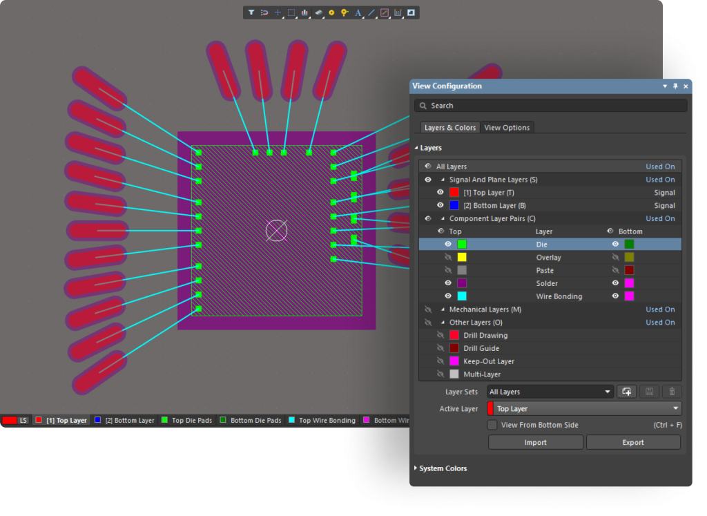
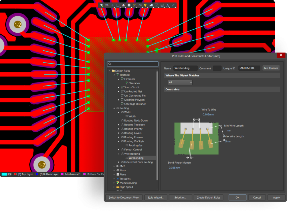
Strona główna » Wire Bonding
Precyzyjne łączenie i efektywne procesy projektowe
dzięki zintegrowanemu wire bonding.
Możliwości projektowania wire bonding w Altium Designer obejmują konfiguracje typu chip-up dla projektów typu Chip on Board (CoB). Dostępne narzędzia oferują elastyczność potrzebną do realizacji tego typu projektów, zapewniając precyzyjne wykonanie i możliwość sprostania wyzwaniom projektowym z pełnym zaufaniem.
Utrzymanie najwyższych standardów dzięki kompleksowym kontrolom weryfikacyjnym. Altium Designer zapewnia zgodność wszystkich połączeń bondingu z rygorystycznymi regułami projektowymi, zapobiegając błędom i zapewniając możliwość produkcji. Automatyczne sprawdzenia DRC weryfikują odstępy między drutami, długość drutów oraz integralność połączeń, zapewniając niezawodne rezultaty projektowe.
Utilize electrical layers outside the main layer stack specifically for die pins and bond wires. This configuration ensures clear and accurate representation of wire bonding elements, enhancing the reliability and precision of your designs.
Podnieś swoje umiejętności projektowe
i usprawnij proces pracy – wszystko pod okiem doświadczonych ekspertów, którzy pokażą, jak w pełni wykorzystać możliwości programu Altium Designer.
Dowiedz się, jak optymalizować połączenia
i projektowanie PCB dzięki funkcji wire bonding.
Jesteś gotowy, aby sprostać wyzwaniom swojej branży?
Skontaktuj się z nami – poznasz nasze rozwiązania i otrzymasz indywidualną poradę od naszych specjalistów. Jesteśmy tutaj, by wspierać Cię w wyborze najskuteczniejszych technologii dopasowanych do Twoich potrzeb.
Świat technologii nie zwalnia. Dzięki naszym rozwiązaniom możesz skupić się na tym, co najważniejsze – na swoim biznesie.