Edytor schematów w Altium Designer jest intuicyjny i przyjazny dla każdego projektanta. Wszystko, co jest potrzebne – projekty hierarchiczne, ponowne wykorzystanie elementów, symulacja i wiele więcej – jest na wyciągnięcie ręki.
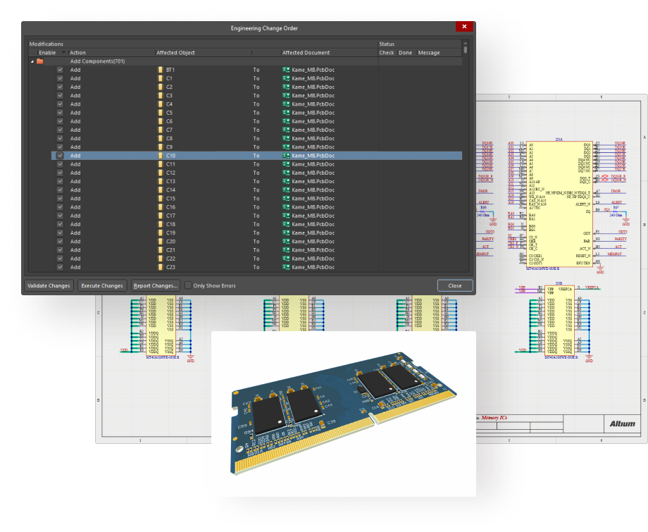
Pełna kontrola nad zmianami między schematem a projektem PCB
W Altium Designer schemat i projekt PCB są dynamicznie powiązane. Dzięki temu unika się problemów produkcyjnych, ponieważ zmiany są odzwierciedlane we wszystkich plikach projektu. Zmiany można przesyłać dwukierunkowo za pomocą kilku prostych kliknięć. Proces aktualizacji odbywa się przez mechanizm ECO, co zapewnia pełną przejrzystość wprowadzanych zmian.
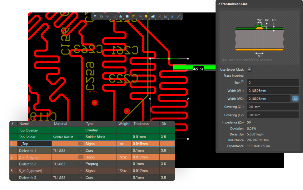
Integracja danych stosu z parametrami elektro-fizycznymi elementów routingu
Tworzenie i edycja stosu warstw PCB w menedżerze automatycznie aktualizuje właściwości elektryczne prowadzenia ścieżek w edytorze PCB. Nowe wartości parametrów są także natychmiast widoczne w menedżerze stosu po dokonaniu zmian.
Key Capabilities
Electrical Layers for Die Pins
and Bond Wires
Utilize electrical layers outside the main layer stack specifically for die pins and bond wires. This configuration ensures clear and accurate representation of wire bonding elements, enhancing the reliability and precision of your designs.
Utilize electrical layers outside the main layer stack specifically for die pins and bond wires. This configuration ensures clear and accurate representation of wire bonding elements, enhancing the reliability and precision of your designs.
Utilize electrical layers outside the main layer stack specifically for die pins and bond wires. This configuration ensures clear and accurate representation of wire bonding elements, enhancing the reliability and precision of your designs.
Utilize electrical layers outside the main layer stack specifically for die pins and bond wires. This configuration ensures clear and accurate representation of wire bonding elements, enhancing the reliability and precision of your designs.
Utilize electrical layers outside the main layer stack specifically for die pins and bond wires. This configuration ensures clear and accurate representation of wire bonding elements, enhancing the reliability and precision of your designs.
Utilize electrical layers outside the main layer stack specifically for die pins and bond wires. This configuration ensures clear and accurate representation of wire bonding elements, enhancing the reliability and precision of your designs.
Utilize electrical layers outside the main layer stack specifically for die pins and bond wires. This configuration ensures clear and accurate representation of wire bonding elements, enhancing the reliability and precision of your designs.
Utilize electrical layers outside the main layer stack specifically for die pins and bond wires. This configuration ensures clear and accurate representation of wire bonding elements, enhancing the reliability and precision of your designs.
Odkryj Pełen Potencjał
dzięki Profesjonalnym
Szkoleniom
Podnieś swoje umiejętności projektowe i usprawnij proces pracy – wszystko pod okiem doświadczonych ekspertów, którzy pokażą, jak w pełni wykorzystać możliwości programu Altium Designer.
Dowiedz się, jak współpracować z zespołem elektryków, nie rezygnując z wydajności i efektywności.
Rozpocznij swój projekt
Jesteś gotowy, aby sprostać wyzwaniom swojej branży?
Skontaktuj się z nami – poznasz nasze rozwiązania i otrzymasz indywidualną poradę od naszych specjalistów. Jesteśmy tutaj, by wspierać Cię w wyborze najskuteczniejszych technologii dopasowanych do Twoich potrzeb.
Używamy plików ciasteczka, aby zapewnić Ci jak najlepsze wrażenia z korzystania z naszej witryny. Więcej informacji dostępne jest w naszej polityce prywatności