Stwórz finalne połączenia
dzięki projektowaniu wiązek przewodów
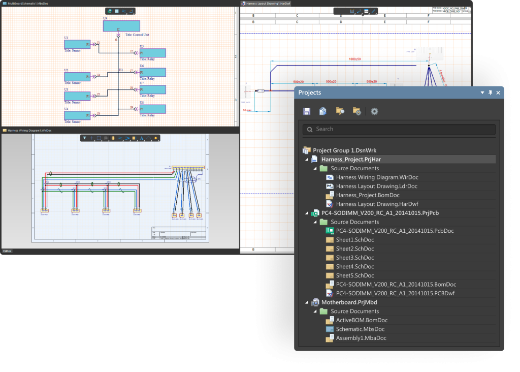
W Altium Designer możesz tworzyć wiązki w znanym środowisku, w którym już projektujesz elektronikę.
Bezproblemowo projektuj połączenia
w wiązkach przewodowych
Bezproblemowe projektowanie połączeń w wiązce
Oszczędność czasu i pieniędzy dzięki funkcjonalności projektowania wiązek, która jest częścią Altium Designer. Nie ma potrzeby kupowania, instalować czy też konfigurowania żadnego zewnętrznego oprogramowania do okablowania czy dokumentacji.
Bezproblemowa integracja z danymi projektu
Praca na jednym, spójnym modelu danych projektu, który unifikuje cały proces projektowy. Łatwy dostęp do szczegółowych danych i ich zarządzania – dla schematów, layoutów, symulacji i projektów wiązek – bez konieczności przechowywania i ręcznej synchronizacji oddzielnych danych dla każdego elementu.
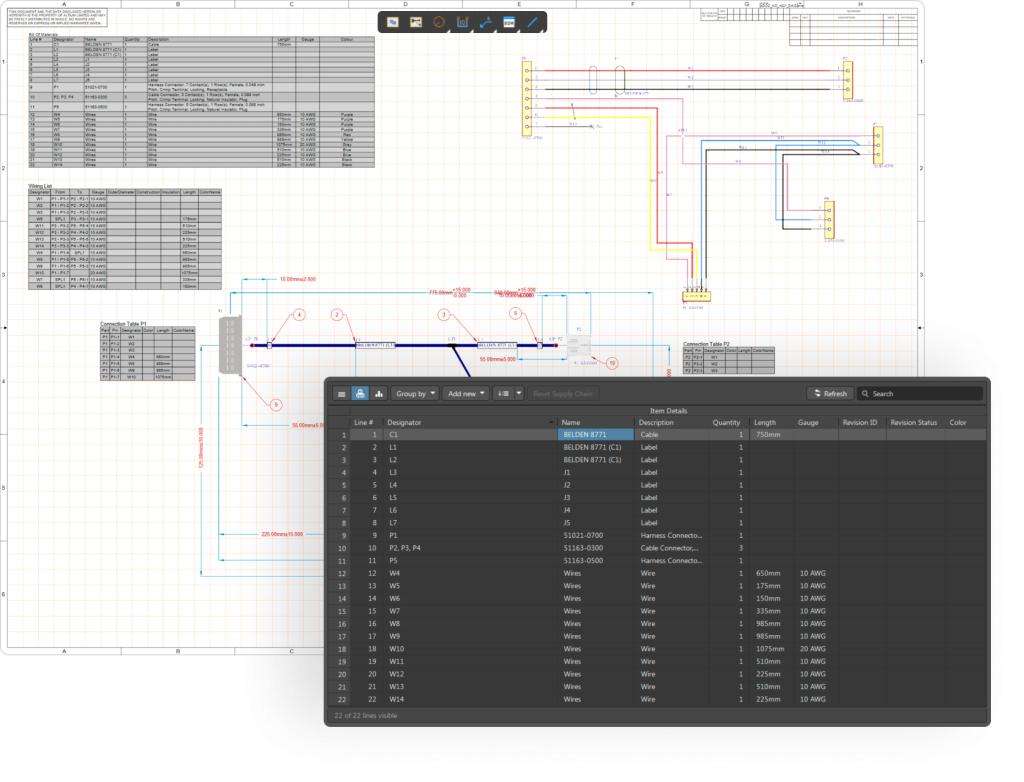
Łatwe przekazywanie wymagań do działów zakupów i produkcji
Możliwość dokładnego śledzenia wyboru elementów dla wiązki i PCB, oraz zapewnienia terminowego montażu urządzenia, poprzez generację BOM oraz rysunków produkcyjnych bezpośrednio w Altium Designer.
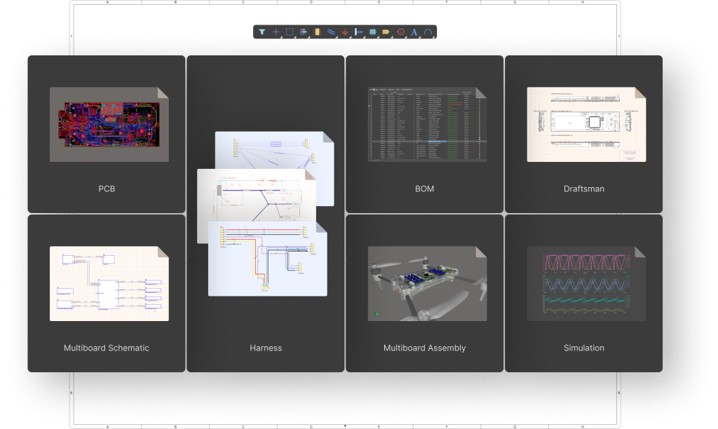
Key Capabilities
Electrical Layers for Die Pins
and Bond Wires
Utilize electrical layers outside the main layer stack specifically for die pins and bond wires. This configuration ensures clear and accurate representation of wire bonding elements, enhancing the reliability and precision of your designs.
Utilize electrical layers outside the main layer stack specifically for die pins and bond wires. This configuration ensures clear and accurate representation of wire bonding elements, enhancing the reliability and precision of your designs.
Utilize electrical layers outside the main layer stack specifically for die pins and bond wires. This configuration ensures clear and accurate representation of wire bonding elements, enhancing the reliability and precision of your designs.
Utilize electrical layers outside the main layer stack specifically for die pins and bond wires. This configuration ensures clear and accurate representation of wire bonding elements, enhancing the reliability and precision of your designs.
Utilize electrical layers outside the main layer stack specifically for die pins and bond wires. This configuration ensures clear and accurate representation of wire bonding elements, enhancing the reliability and precision of your designs.
Utilize electrical layers outside the main layer stack specifically for die pins and bond wires. This configuration ensures clear and accurate representation of wire bonding elements, enhancing the reliability and precision of your designs.
Utilize electrical layers outside the main layer stack specifically for die pins and bond wires. This configuration ensures clear and accurate representation of wire bonding elements, enhancing the reliability and precision of your designs.
Utilize electrical layers outside the main layer stack specifically for die pins and bond wires. This configuration ensures clear and accurate representation of wire bonding elements, enhancing the reliability and precision of your designs.
Odkryj Pełen Potencjał
dzięki Profesjonalnym
Szkoleniom
Podnieś swoje umiejętności projektowe i usprawnij proces pracy – wszystko pod okiem doświadczonych ekspertów, którzy pokażą, jak w pełni wykorzystać możliwości programu Altium Designer.
Dowiedz się, jak współpracować z zespołem elektryków, nie rezygnując z wydajności i efektywności.
Rozpocznij swój projekt
Jesteś gotowy, aby sprostać wyzwaniom swojej branży?
Skontaktuj się z nami – poznasz nasze rozwiązania i otrzymasz indywidualną poradę od naszych specjalistów. Jesteśmy tutaj, by wspierać Cię w wyborze najskuteczniejszych technologii dopasowanych do Twoich potrzeb.
Używamy plików ciasteczka, aby zapewnić Ci jak najlepsze wrażenia z korzystania z naszej witryny. Więcej informacji dostępne jest w naszej polityce prywatności